Our products are designed to solve inspection requirements in the field of semiconductors, microelectronics, optics, and surface finishing. Covering the large markets of precision manufacturing and consumer electronics.
Batteries Display IC Packaging Medical Implants
Optics PCB Semiconductors Tooling
All applications
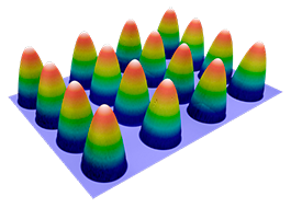
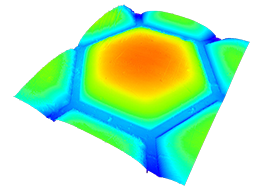
In our increasingly electrified world, batteries play a pivotal role in powering everything from electric vehicles to portable electronics. Sensofar’s /Non-contact 3D optical systems /are ideal for measuring surface texture, flatness, and critical dimensions of batteries, providing crucial insights for enhancing battery efficiency, lifespan, and safety.
All applications
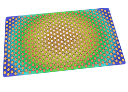
We work mainly with FPDs (Flat Panel Displays) to measure different features -arrays, coatings, or spacers- depending on which stage of the manufacture the characterization is performed.
All applications
Integrated Circuit (IC) Packaging is the last stage of semiconductor manufacture and consists of the encapsulation of a semiconductor component. We mainly measure the dimensions of the pins and their surface finish so they connect properly to the PCB.
Medical Implants
All applications
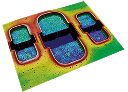
Ensuring the highest quality standards is crucial in medical implants, where precise assessment tools are essential for predicting outcomes. Sensofar’s optical systems provide reliable characterization of surface texture, volume, and critical dimensions of medical implants, delivering tailored solutions to meet the specific demands of various applications.
Optics
All applications
The optics application is known to be a challenging one: samples are very smooth, flat, and sometimes transparent. Only high-end profilometers can image them and meet the tight requirements this field demands. Our experience is in lenses and optical filters for roughness, arrays of micro lenses, and film thickness.
All applications
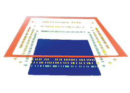
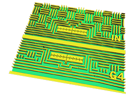
Manufacturing PCBs can vary greatly depending on the purpose and design of the board. Nevertheless, there are common elements that apply to all PCBs that are critical for their correct function. Sensofar has optimized its analysis software to copper circuits, vias, and pads.
All applications
For semiconductor applications, Sensofar’s products can characterize critical dimensions, roughness, and perform defect inspection, frequently within the back-end packaging of the manufacturing process.
All applications
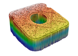
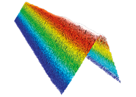
Characterizing cutting tools is very important to ensure a quality final product. It can also give information about the amount of material that will be removed when cutting. More specifically, the cutting edge of a tool is a key feature to characterize, in terms of useful lifespan and performance of the tool and the required speed and resulting precision of the cut.


